When I first learned about a material called silicon carbide, it blew my mind. It is one of the hardest synthetic materials, nearly as hard as diamond, and difficult to corrode. Its inner structure can take the form of more than 200 different crystal types. And here's the really cool part: at atmospheric pressure, it never melts—when it reaches 2,700 degrees Celsius, it skips a liquid form and turns straight from a solid into a gaseous vapor.
I was working toward my Ph.D. in mechanical engineering at the University of California, Berkeley, when I encountered silicon carbide, and its unreal properties got me hooked on materials science. I was inspired to investigate the challenges and opportunities of using this strange material to make electronics.
Only after I earned my Ph.D. did I learn that silicon carbide wasn't just tough on Earth—it could also withstand many of the extraordinary conditions found in space: radiation, space dust, wild temperatures and a lack of gravity. Cosmic radiation—high-energy particles such as protons, electrons and neutrons—degrades most electronics. But silicon carbide is 60 percent less sensitive to cosmic rays than silicon. And most materials can't handle the temperature extremes of, say, scorching Venus or frigid Uranus, let alone swing between such opposites. But silicon carbide can.
Realizing that silicon carbide might have the right properties to work in space set the direction for my career, which combines materials studies with space exploration. I'm fascinated by how space affects materials and how materials perform in space. Today I design electronics to fly on space missions and study how growing materials in orbit can improve them.
Most of my work has focused on Venus. It's our closest neighbor, but humans have glimpsed only a handful of color panorama images of Venus's surface, taken during a Soviet mission in 1982. Scientists hypothesize that billions of years ago Venus looked like Earth, with flowing water and a cooler climate. Today its surface burns at 475 degrees C, hot enough to melt lead. The atmosphere is filled with carbon dioxide and sulfur dioxide, and sulfuric acid rain clouds cover the skies. Venus has crushing pressure at its surface—more than 90 times that of Earth—similar to the pressure you'd encounter a mile below the ocean here.
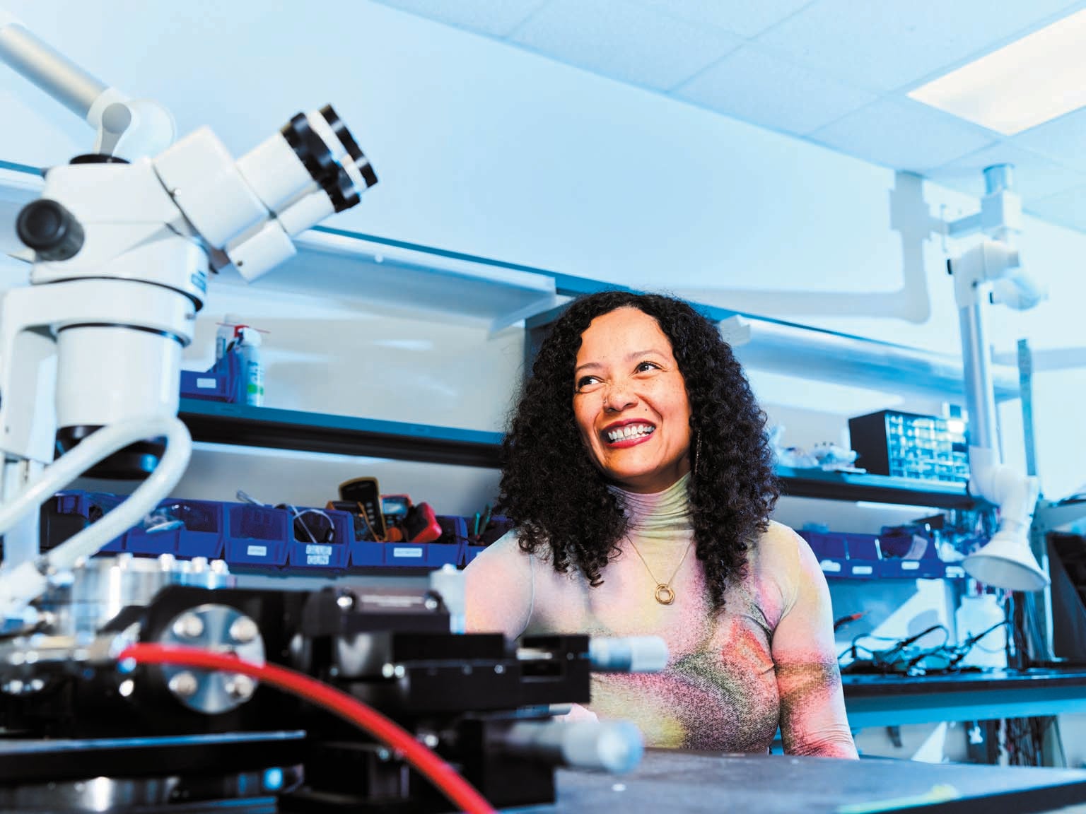
I would love to see, in my lifetime, a lander mission to Venus that could collect dynamic data about surface temperature and weather patterns. NASA has proposed conducting a 60-day mission to take a range of measurements from Venus's surface, but the agency doesn't yet know how to build the necessary instruments. At my EXtreme Environment Microsystems Laboratory (XLab) at Stanford University, my students and I construct tiny but tough electronics designed to survive everything Venus will throw at them.
Venus's high temperatures are among the biggest hurdles. Under that kind of heat, many materials will simply melt. Even if they don't, their elasticity and other properties can change, and it's hard to predict how these shifts will affect the materials' ability to function. If your cell phone, for instance, landed on Venus, the thermal energy would set off a flurry of electrons and send your device on the fritz.
Cell phones (and most of our everyday electronics) rely on semiconductor materials, primarily silicon. These are usually layered with a metal electrode on top. But when they get too hot, the metal can diffuse into the semiconductor material and turn it into an undesirable alloy, changing the material's mechanical and electrical properties.
This is where silicon carbide comes in. It and another material I study called gallium nitride are good alternatives to regular silicon. Gallium nitride is often used in power electronics, high-frequency electronics and blue LEDs. Both materials have semiconducting properties like silicon, but unlike silicon, they can also withstand high temperatures and radiation because of their wide electronic bandgap and high atomic binding energy. In simple terms, it takes a lot of energy for electrons to reach the level required for conduction in these materials, so they maintain their normal conductivity even when hot. Gallium nitride can electrically function at temperatures higher than 1,000 degrees C.
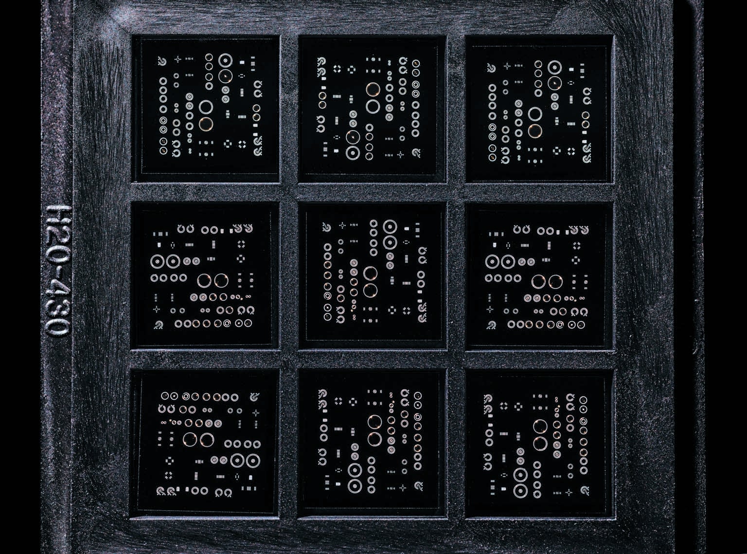
In the clean rooms at the Stanford Nanofabrication Facility, my students and I build tiny gallium nitride transistors. Next we bring them over to the XLab, where we keep them heated to 470 degrees C for six days with our specialized testing equipment. Six days isn't as long as 60 days, the length of the planned NASA mission to Venus, but it's a lot longer than the two-hour mission the Soviets made 30 years ago, so we're headed in the right direction.
Sometimes we further subject our electronic components to the full simulated chemical experience of Venus in NASA's Glenn Extreme Environments Rig in Cleveland. Some of my experiments have used this facility, experiencing a temperature of 475 degrees C along with the sulfur dioxide and 90-bar pressure present on Venus. I don't want to have that kind of acidic chemistry in my lab, but I'm glad NASA does.
As promising as silicon carbide and gallium nitride are for making extraordinarily resilient electronics, they are difficult to manufacture on Earth without a lot of defects—we can make only small wafers of them here. The situation might be different, however, in space, where the absence of several gravity-based phenomena should enable us to grow larger, more uniform crystals and other materials faster.
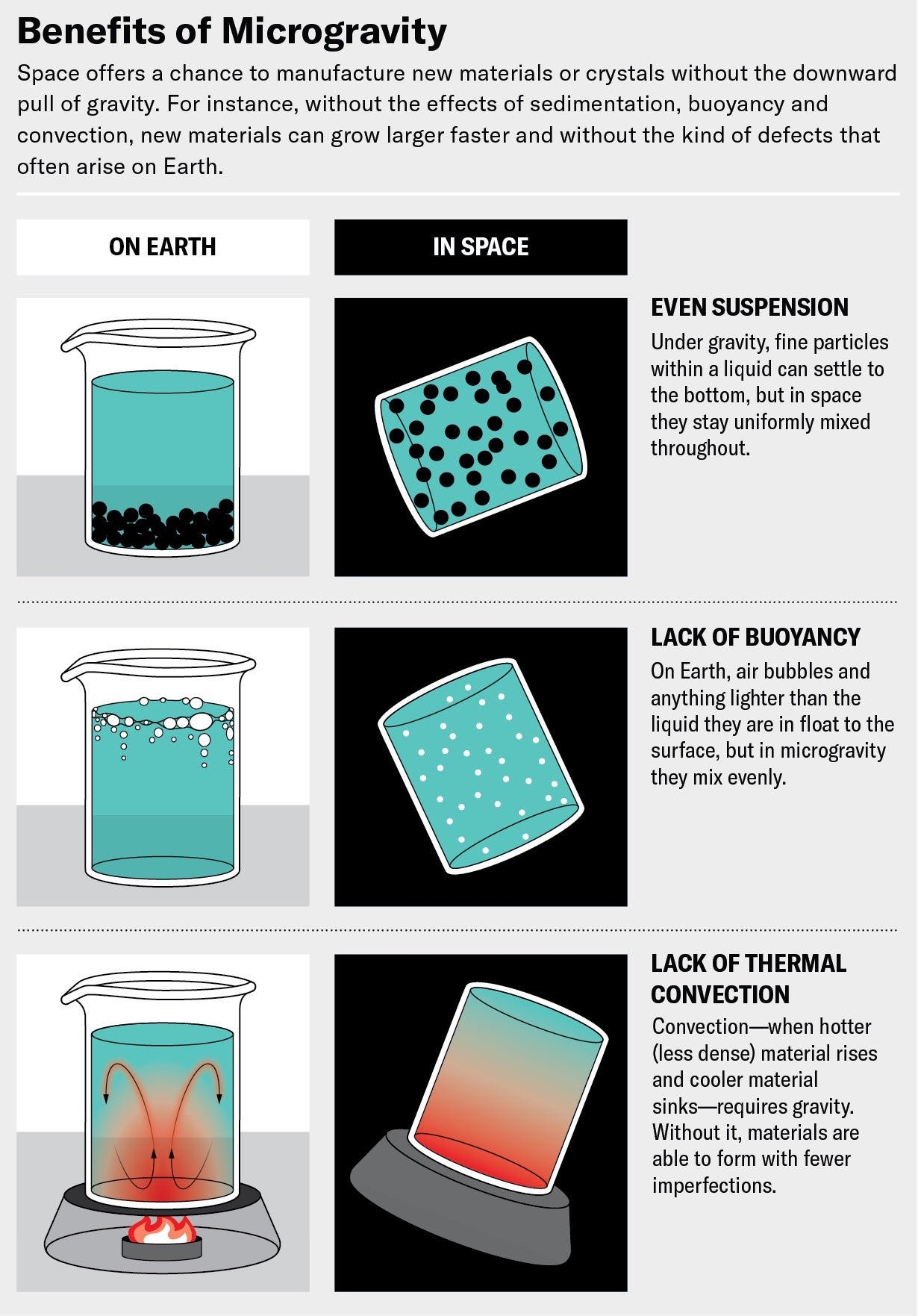
Here on Earth gravity limits the physics we rely on to construct semiconductors and other materials. Making materials without gravity offers a kind of freedom. To understand the difference, consider a cup of Turkish coffee on Earth. After gravity drags the fine coffee grounds to the bottom of the cup, you can drink your unclouded coffee from the top. But in the microgravity of space, Turkish coffee grounds would float evenly throughout the cup, and an astronaut taking a sip would end up with a mouthful of fine particles. Inconvenient for drinking coffee, sure, but beneficial for other purposes. When substances are suspended evenly within a fluid, as they are in space, we can engineer materials with more uniform properties and do so at a faster pace.
Another limiting factor on Earth, buoyancy, is absent in microgravity. Here air bubbles and other substances lighter than water float up through the liquid. When you synthesize a material on the ground, buoyancy can stop two substances from mixing evenly. But in microgravity, an air bubble weighs the same as water and won't rise to the surface, so the water and air mix better.
Thermal convection—the movement of particles in a fluid or gas caused by temperature changes, which can disrupt material synthesis and harm the quality of the end product—is yet another process that doesn't occur in microgravity. As a result, materials made in microgravity without convection show fewer imperfections.
I first became interested in growing materials in orbit about five years ago, when I was invited to a workshop to discuss nanomaterials fabrication in space. I didn't have much expertise in the topic, but the event piqued my interest. After the workshop, there was a call for proposals to manufacture materials on the International Space Station (ISS), and I jumped at the chance. The opportunity was a joint solicitation by the National Science Foundation and the Center for the Advancement of Science in Space (CASIS), which manages the space station and research conducted there.
Up to that point I'd known how to make things only on Earth. Getting up to speed felt like a return to my graduate student years. For several days I stayed up all night reading papers about past work on the space station. The more I learned, the more excited I got about manufacturing in microgravity. It was like a lightbulb turned on in my mind—I knew microgravity was the new frontier for semiconductors and materials science.
Not only could materials made in space be superior to those made on Earth, but they also could be preferable for eventual use in space: making them there is certainly more convenient than building everything on Earth and schlepping it up on a rocket. When one of the ISS crew members lost a wrench somewhere on the spacecraft in 2014, for instance, engineers uploaded the first 3-D-printer design to space and built the astronaut a replacement wrench right there.
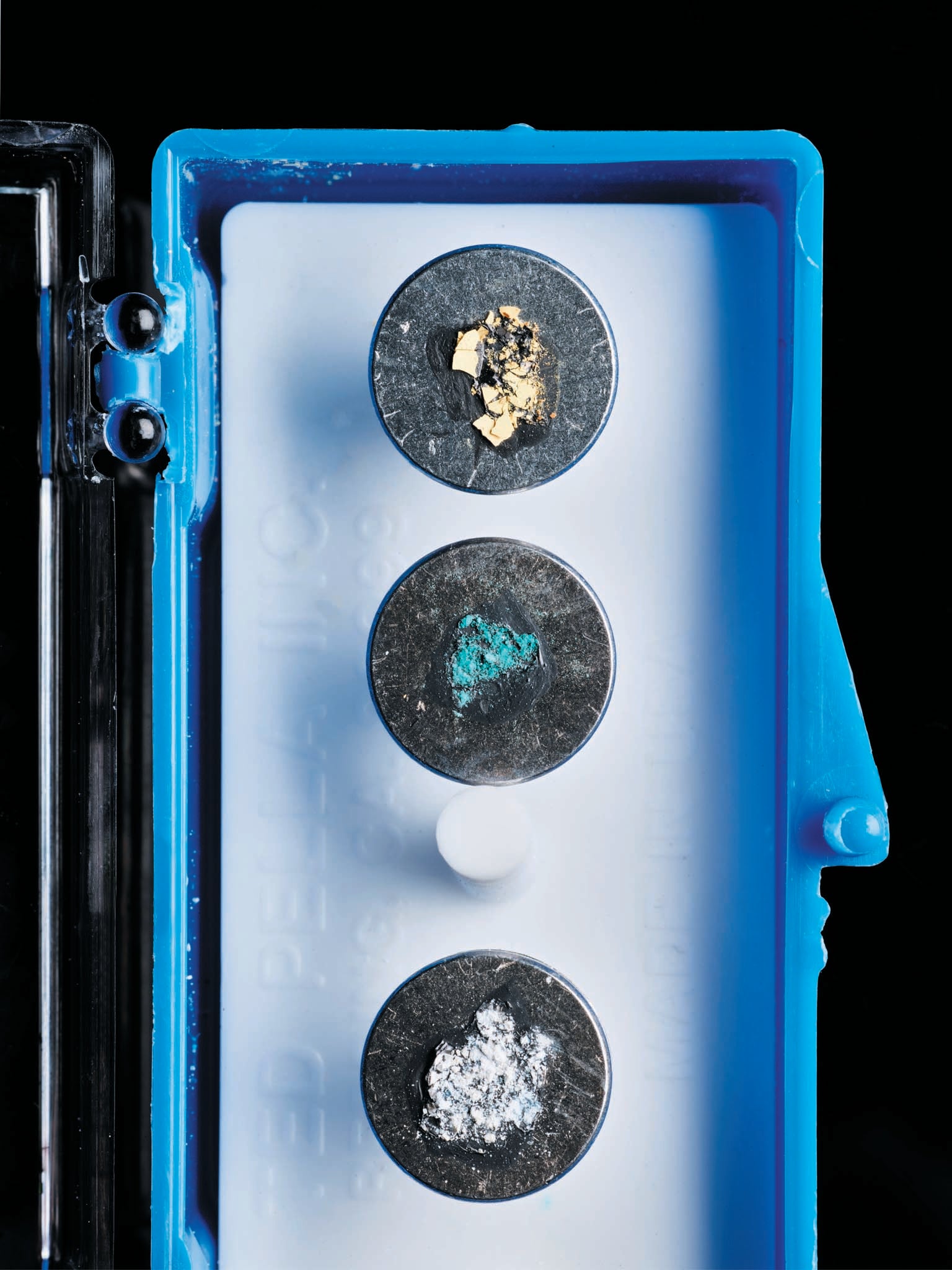
When I started studying this subject, I had no clue that NASA scientists had already made semiconductor crystals in space. In 1992 NASA launched the first U.S. Microgravity Laboratory onboard the space shuttle Columbia, and there astronauts produced two crystals of a material called gallium arsenide. More recently, scientists have made fiber-optic cable materials in space that can transmit lasers and Internet signals with enhanced clarity. After getting up to speed, I devoted myself to designing my own experiment for space. One of the challenges was figuring out what tools I had access to on the station. Making semiconductor crystals or materials often requires high temperatures, which can be dangerous. Most of the equipment on the ISS is tailored for biology experiments that run at cooler, safer temperatures. Luckily for me and my team, there is a small machine onboard called the SUBSA (Solidification Using a Baffle in Sealed Ampoules), akin to a furnace that you would see in a semiconducting clean room. It can reach 850 degrees C—plenty hot for our purposes.
My collaborators and I came up with the idea to grow a type of nanomaterial, a graphene aerogel, in the SUBSA furnace, and we won the NSF-CASIS award.
We triumphantly launched our experiment to the ISS onboard the Northrop Grumman NG-19 rocket on August 1. We sent a small autoclave—a machine that creates elevated temperatures and pressures—filled with water and flakes of graphene oxide, which we use as a starting ingredient. After it arrived, astronauts loaded the autoclave into the SUBSA furnace and turned the heat up to 180 degrees C. During this process the contents were converted into graphene hydrogel—basically a mixture of graphene and water. These samples are now back on the ground, having returned on September 4 via SpaceX's Crew-6 mission. It's exciting to think that our experimental products reentered Earth's atmosphere alongside four astronauts. Now we plan to dry the samples out to change the hydrogel into an aerogel, in which the water is replaced by air.
Graphene—a one-atom-thick sheet of carbon bonded in a hexagonal structure—is stronger than steel and is electrically conductive. When it's in the form of graphene aerogel, it's a bit spongy and has properties that could make it useful for lots of applications: thermal insulation, energy storage in batteries, environmental protection materials, sensing materials, and more.
When we make graphene aerogel in my XLab here on Earth, gravity can disrupt the way sheets link together during the process of becoming a gel. Plus, the material is prone to sedimentation. Graphene flakes can sink to the bottom of our container like the Turkish coffee grounds. This imbalance can lead to aerogels with less uniform conductivity, creating hotspots and failures.
But my students and I expect that on the ISS the flakes will float freely. We predict that we'll end up with a more even structure and uniform properties when sedimentation and buoyancy forces aren't in play. The end product might be able to insulate heat more uniformly across an area, for instance. In addition, our aerogel could serve as an electrode that has a more regular density of current, eliminating hotspots. We expect that batteries designed with this space material would run more reliably. Common metal electrodes suffer from swelling when they go through charge-discharge cycles; they fracture and break. Spongelike graphene aerogel reduces those potential breakages.
Now that we have our payload back from space, we'll look at the structure of the aerogel that we produced. We'll measure its mechanical, thermal and electrical properties and compare them with the properties of aerogels made on the ground. I'm curious about whether we'll see interesting shapes form in the microphysical structure of the space-grown aerogel, for example. When I zoom in on a conventional graphene aerogel with a scanning electron microscope, the structure looks very porous and tortuous, and the sheets are randomly bound together. I wonder whether we're going to see a more periodic structure, something more repeatable, in the sample made in microgravity.
If these space-made aerogels do grow more evenly and perform better than their terrestrially produced counterparts, they could be the building blocks of sensors, batteries and thermal insulation for future spacecraft.
Our experiment on the ISS is just a beginning. We hope it will help show that we can make superior materials in microgravity. Next we'll grow more types of materials that prove challenging or impossible to synthesize here. Our latest research program is focused on growing metal organic framework crystals in prolonged microgravity. In addition to discovering new materials, we'll also need to increase the size of our experiments and integrate the materials we make into actual products to be used on Earth. The diameter of the container we sent to the space station measures a mere five millimeters. If we want to produce larger materials for practical purposes, we'll eventually have to move beyond the ISS to a station dedicated for production, such as one of the free-flying commercial space stations being planned for the late 2020s.
I'm surprised more people aren't more excited about this potential. People in the semiconductor industry should start seriously considering mass-producing their products in space. They currently must toss out lots of material that contains defects. Without this waste they could possibly cover the cost of building factories in orbit. We could see semiconductors mass-produced with higher performance, reliability and scalability than we can achieve on Earth.
With the growth of the commercial space industry, we're soon going to see more frequent missions and more human activity in orbit. Industry should plan to piggyback on that ride. Factories in space may sound like science fiction, but I believe they should be a part of our everyday life. I'm thrilled that the work coming out of my lab will help move us toward that dream.